


Inside TSMC, the $1 Trillion Ghost Foundry Behind Nvidia's Crown
How a chip factory powers every AI boom, and the future‑ready playbook no business can ignore.


Late one evening in 2010, in his Taipei home, Morris Chang topped off the wine in his guest’s glass. Across from him sat Jeff Williams, Apple’s chief operating officer, who had flown in with a proposal that was as audacious as it was simple.
Williams got straight to the point: We want to move the iPhone’s chipmaking to TSMC, but on a production line so advanced it existed only on paper.
TSMC had just poured billions into perfecting its current 28‑nanometer process, circuits roughly one‑ten‑thousandth the width of a human hair. Apple was asking for 20 nm, an even tighter scale that wasn’t on TSMC’s roadmap.
Saying yes meant undertaking a frantic, high-stakes race to build new capacity from scratch. But CEO Morris Chang did not flinch. He listened calmly as Williams spoke. (By Chang’s own count, the Apple exec did 80% of the talking that night.)
Chang later told his team that “Missing Apple would cost us far more,” as he authorized a crash program to build the new production line. It’s a gamble of nearly half of TSMC’s cash reserves: A $9 billion investment, with 6,000 people working around the clock. In a record 11 months.
“I bet the company, but I didn’t think I would lose,” the CEO said.
That single decision, to go all-in for Apple, would rewire the entire semiconductor industry. It changed everything.
Fifteen years later, at 9:32 AM on July 9, 2025, the unthinkable flashed across trading desks worldwide: NVIDIA — a company once known only for its video-game graphics chips — had just dethroned Apple as the world’s most valuable company, with a staggering $4 trillion market cap.
On Wall Street, traders whooped and headlines blared. Half a planet away in Taiwan, inside a humming TSMC fab, engineers in cleanroom suits stayed focused on their monitors. No applause, no champagne, just the steady whir of machines laying down atoms on silicon wafers. They didn’t need to cheer. The milestone had been engineered long ago.
By July 2025, Taiwan Semiconductor Manufacturing Co. (TSMC) had quietly grown into a trillion-dollar colossus itself, firmly in the world’s top ten by market value, well ahead of stalwarts like JPMorgan and Walmart and Visa.
Worth barely a tenth of that was Intel, once the chip industry’s lodestar. All these were the direct result of a paradigm that TSMC had been forging for more than a decade.
In an age where politicians clamor to bring manufacturing “back home,” the truth is more complicated, and more inspiring. TSMC isn’t just a factory. It’s Nvidia’s factory. And Apple’s. And Qualcomm’s. And AMD’s. It’s the silent partner behind every AI boom headline. The ghost in the machine. The engine inside the engine.
This is the story of how making microchips became a team sport. How the old model of one company doing it all, like Intel’s proud in-house empire, was outpaced by a new era of openness, partnership, and focus.
It’s the story of how the tech world was unbundled. How one kingdom fell, and another rose in its place. Because the biggest breakthroughs didn’t come from working in isolation. They came from borderless collaboration.
It challenges the very notion of what a company should be. It reveals a future-ready strategy that no business, in any industry, can afford to ignore.
I. The Fortress of Solitude: Intel's Gilded Cage (1968–2005)
When Gordon Moore and Robert Noyce founded Intel in 1968, they fused physics brilliance with manufacturing might under one roof. The model was singular and uncompromising: one team, one mission. Design engineers sat just meters away from fabrication experts. Problems were solved over cafeteria coffee. Secrets never leaked. Everything — from transistor layout to atomic-level etching — stayed in-house.
By the 1990s, Intel was in the PC era. Its microprocessors powered over 90% of the world’s personal computers. “Intel Inside” became a consumer-facing brand, not just a sticker on a laptop, but a seal of dominance.
The strategy was simple yet profound: own the whole stack. Intel controlled every stage of production.
It poured billions into R&D.
It hired the sharpest minds in the Valley.
It relentlessly pushed Moore’s Law (doubling transistor density every two years).
And it worked.
Competitors like AMD survived on scraps. Intel’s vertical integration made it a juggernaut. It was the Roman Empire of tech: self-sufficient, all-knowing, seemingly invincible. By the year 2000, Intel’s market cap peaked around $500 billion, more than the GDP of Sweden. CEO Andy Grove’s mantra, “Only the paranoid survive,” became gospel in boardrooms and business schools alike.
Intel’s Santa Clara campus wasn’t just a workplace; it was a fortress. But then it became a cage.
II. The Great Unbundling (2005–2016)
In 2007, Steve Jobs made an offer to Intel to power the first iPhone. We're building a new kind of phone. Want in?
Intel’s CEO at the time, Paul Otellini, did the math. The chips would be low-margin. The volumes looked small. Intel was printing money with PC processors.
Otellini said no. “We didn’t think it would be high volume.” That single misjudgment would haunt Intel for years. Apple turned instead to ARM-based chips. That’s why Jeff Williams flew across the Pacific to see Morris Chang.
When Intel hesitated, TSMC listened. And with that, the old empire began to crack.
The architect of this new world wasn’t your typical hotshot founder in a hoodie. Morris Chang was 55 when he returned to Taiwan, an elder statesman in an industry infatuated with youth.
Armed with an MIT PhD and 25 battle-hardened years at Texas Instruments (TI), Chang had seen it all. At TI, he had championed a radical strategy known as “ahead of the cost curve”: sell chips below their current cost to lock in future demand. Audacious. Borderline reckless. But it worked.
Chang drove down costs faster than competitors could react.
His goal was to “sow despair in the minds of my opponents.”
TI’s fabs ran at full tilt. The semiconductor division boomed.
But by the early ’80s, TI’s focus had shifted to consumer electronics. Chang was passed over for CEO. So at 55, he left the U.S. and returned to Taiwan. He was recruited by the government to do something few thought possible: build a national tech industry from scratch.
The Veteran with a Radical Idea
Chang had watched too many brilliant engineers fail to launch semiconductor startups because they couldn’t afford their own fabs. Capital outlays often ran over a billion dollars, even back then.
So he flipped the model.
Chang launched Taiwan Semiconductor Manufacturing Company (TSMC) in 1987 with a pledge: We will never compete with our customers.
TSMC would make chips and chips only. It wouldn’t design them. It wouldn’t release rival products. It would be a pure-play foundry, like a printing press for silicon. He also received zero equity as a founder. Every penny of his eventual $3 billion net worth came from buying shares with his own salary.
According to a recent survey, 64% of professionals feel overwhelmed by how quickly work is changing, and 68% are looking for more support to keep up. If you enjoyed this article and it brought you clarity, could I ask a quick favor?
Subscribe now. It’s free and takes just seconds to sign up.
You’ll join thousands of other ambitious managers and CEOs getting exclusive, research-backed insights straight to their inbox. Let’s keep you one inch ahead.
The genius of the model lay in its ability to pool risk. By serving hundreds of customers — Apple, Nvidia, AMD, Qualcomm, and more — TSMC could keep its multi-billion-dollar fabs running near full capacity all the time. One customer’s flop would be offset by another’s blockbuster. TSMC didn’t need to predict the winners; it just had to be the best at serving all of them. Rather than bet on which chip would succeed, TSMC would bet on all of them.
Unlike Intel’s walled garden, TSMC’s model was built on radical openness:
Manufacture only others’ designs.
Share process secrets and tools with partners.
Pool demand across competitors, filling fabs around the clock.
That was the Great Unbundling, trading fortress-like empires like Intel for a sprawling, open ecosystem led by TSMC.
III. A Day in the Life of the Borderless Chip
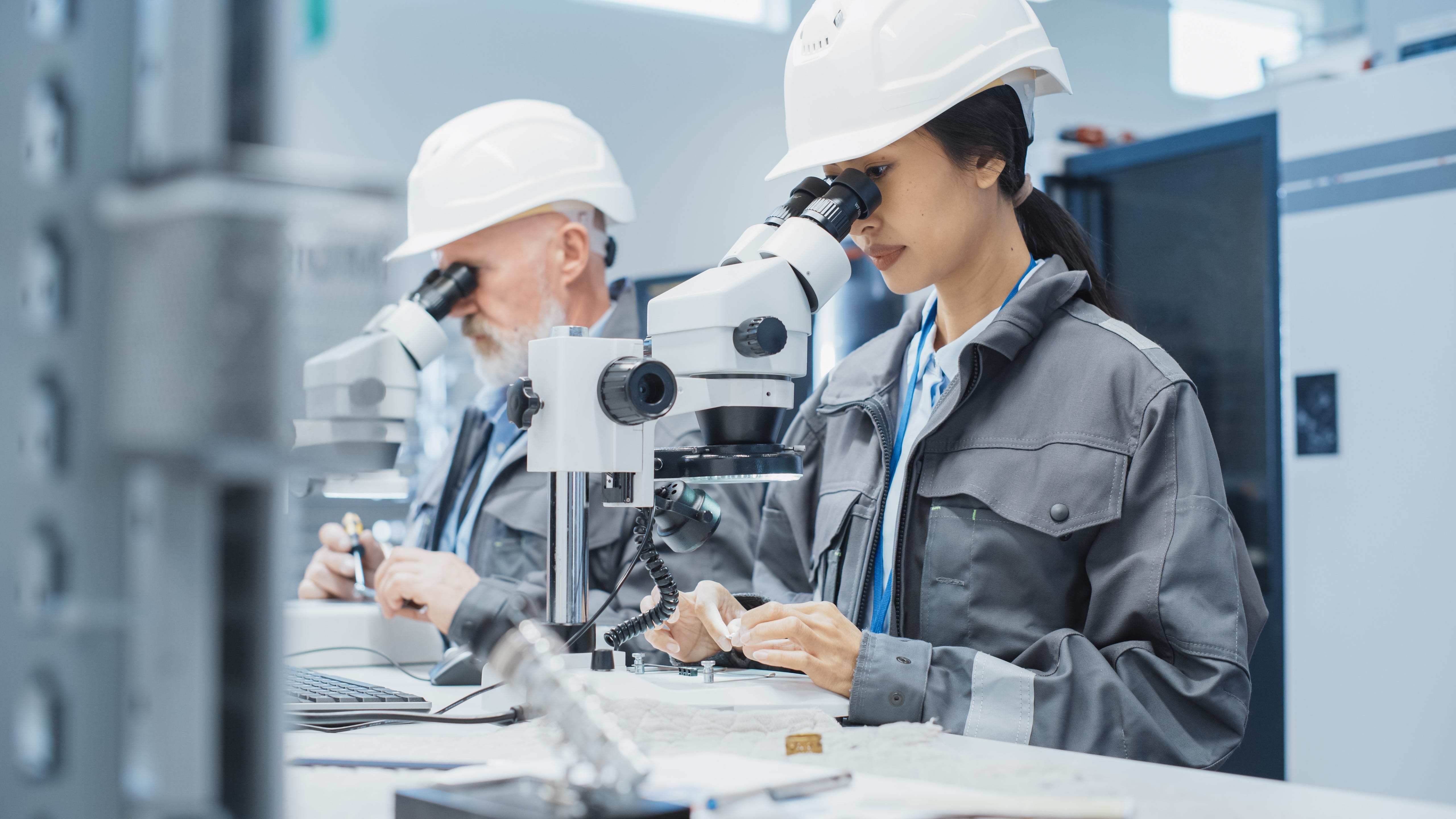
To understand how this borderless chip empire actually works — how a company in California can build the most advanced hardware on Earth without ever touching silicon — you have to meet a chip designer. Let’s call her Anna.
Anna is a senior engineer at a fabless company like Apple or Nvidia. Her task: design a next-generation AI accelerator. Her challenge: cram more computing power into a smaller chip that draws less energy, and ship it before competitors even start thinking about it.In 2025, Anna’s most important collaborators aren’t down the hall. They’re 13 time zones away, inside a fabrication facility she’ll likely never visit. That’s why Anna’s workspace isn’t a lab bench or a cleanroom. It’s a virtual cockpit.

There, she operates a suite of high-powered digital tools — streamed securely from TSMC’s servers in Hsinchu — forming a kind of chip design metaverse. Among them:
The Rulebook (Design Rules)
Every chip designer at TSMC must follow a massive list of do’s and don’ts. These rules cover tiny details, like how close wires can be, or how much electricity each part can handle. If you break just one rule, the chip might not work at all.
This rulebook is like a secret recipe, capturing everything TSMC has learned about making world-class chips.
The LEGO Bricks (Standard Cells)
Instead of building every tiny part from scratch, designers use ready-made building blocks. These blocks—like memory bits or logic gates—are tested, reliable, and designed to fit together perfectly.
It’s like building something complex out of LEGO: faster, safer, and way less likely to break.The Crystal Ball (Simulation Models)
Before a chip is ever built, designers use powerful software to predict exactly how it will perform. They can see how fast it will run, how much energy it will use, and how hot it might get.
It’s like taking the chip for a test drive, without having to build it first. Because if something goes wrong after it’s built, fixing it can cost millions.
It’s past midnight. Anna rubs her eyes as lines of code blur on the screen. A simulation error blinks red. Her stomach knots. One more problem to solve before dawn.
She tweaks a tiny circuit parameter, heart pounding. Then the red alert flickers to green.
Anna exhales. A small smile cuts through the fatigue.
The Unsung Heroes of Automation
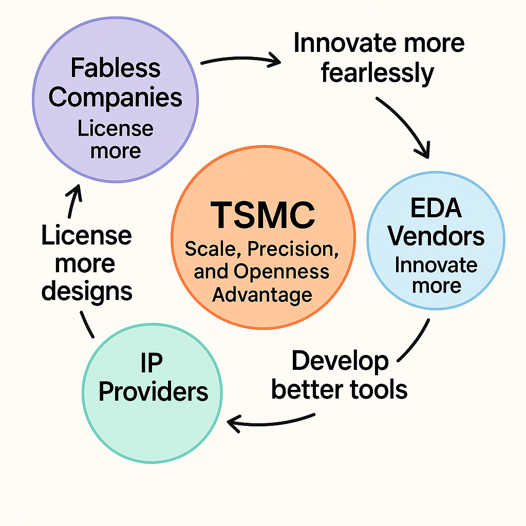
TSMC didn’t create the chip design metaverse on its own. Since 2008, its Open Innovation Platform (OIP) has been the glue binding together a powerful alliance of key players:
IP core providers like ARM, who license ready-made building blocks used in chips. Things like CPU cores, graphics engines, and communication controllers.
EDA (Electronic Design Automation) vendors like Synopsys and Cadence, who provide the software tools that help engineers design and test chips with billions of tiny components.
EDAs? Let’s pause. No story of unbundling is complete without these unsung heroes.
Back in the mid-1980s, a team led by Aart de Geus spun out of General Electric to found Synopsys. Their breakthrough? Logic synthesis. A software tool that could take a high-level description of a chip’s intended behavior and automatically generate an optimized circuit layout.
At first, customers were skeptical. Could a machine really do better than human engineers? But the results were undeniable: Designs that once took months could now be synthesized in weeks, often with fewer errors.
Meanwhile, a startup called ECAD (which later merged into Cadence) developed tools that could automatically verify chip layouts with blazing speed. Together, these tools democratized chip design.
Welcome to the Great Library of Taiwan
Today, through TSMC’s OIP, players like Synopsys, Cadence, and IP vendors start working together years before a new chip process is even ready. So by the time engineers like Anna show up at TSMC:
The design tools are already fine-tuned and certified for the latest tech.
The simulation flows have been road-tested to catch expensive mistakes.
More than 60,000 plug-and-play chip components, all proven to work in real silicon.
It’s like stepping into the Great Library of Taiwan, where every book, every IP block, is guaranteed to function flawlessly at the 3-nanometer scale.
(Fun fact: TSMC’s 3nm transistors are so small that if you blew one up to the size of a marble and blew a regular marble proportionally, the regular marble would be about the size of Earth.)
Even the heaviest simulations now run seamlessly in the cloud — on AWS or Azure — thanks to TSMC’s Virtual Design Environment (VDE). Once, this kind of computing firepower was reserved for the likes of Intel. But now, it’s available to anyone with ambition, and a login.
What’s work like for Anna? It’s as if she’s working inside TSMC, without ever leaving California. This isn’t outsourcing. It’s deep entanglement.
IV. The Reckoning
Intel’s decline wasn’t a dramatic collapse. It was a slow, grinding erosion.
First, it missed the smartphone wave entirely. Then came a misfire: betting big on its own low-power Atom chips that never caught on. Meanwhile, its greatest strength — manufacturing — began to falter. The once-reliable cadence of process improvements slipped. Intel’s long-promised 10nm node arrived years late.
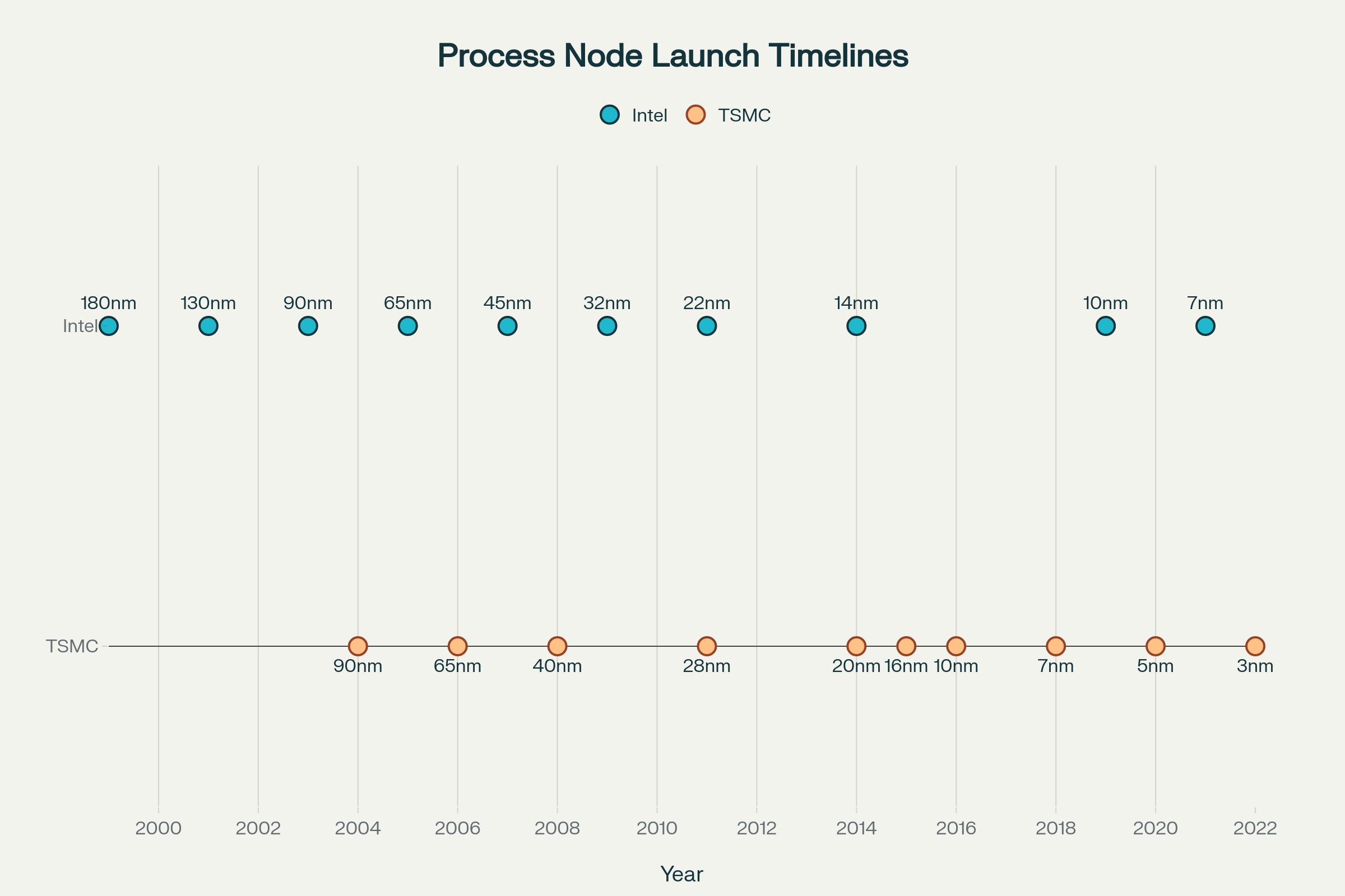
By contrast, TSMC advanced in lockstep with its partners, moving like a steady metronome.
7nm in 2018, powering Apple’s A12 and Huawei’s Kirin chips.
5nm by 2020, for Apple’s A14 and the first M1 Macs.
3nm by 2023, arriving on time, on target.
By the time Washington realized America’s chip supply rested on an island just 100 miles from China, it was too late. The geopolitical alarm bell rang. The response was massive: $6.6 billion in CHIPS Act grants and another $5 billion in loans to lure TSMC into building fabs in Arizona.
Building factories is easy. But replicating excellence? That’s hard.
Taiwan’s 24/7 Discipline Meets America’s 9‑to‑5
By 2024, TSMC’s U.S. operations were deep in the red, posting a staggering NT$14.3 billion loss (roughly USD $440 million). The Arizona fab, once hailed as a symbol of industrial revival, had become TSMC’s most costly site.
The problem wasn’t technology. The chips scheduled to come out in 2025 were still world-class. The problem was culture.
The precision required in semiconductor fabrication defies comprehension. Extreme ultraviolet (EUV) machines fire lasers that must hit droplets of molten tin 50,000 times per second. That’s an accuracy exceeding the math used in Apollo moon landings.
But the cultural misalignment was harder to control than any beam.
Inside the Arizona project, a clash of norms played out. American engineers chafed under at what they saw as “rigid, counterproductive hierarchies. Some found the environment “prison-like.” Decisions flowed strictly top-down. Overnight shifts and 12-hour days weren’t just common, they were expected. What Taiwanese leadership saw as discipline, U.S. staff saw as dysfunction.
Taiwanese managers, meanwhile, were dismayed by what they perceived as a lack of “dedication and obedience.” American engineers seemed overly fixated on work-life balance, unwilling to push through the kind of relentless all-hands grind that TSMC’s culture had long normalized.
In Taiwan, manufacturing is treated with the urgency of a national mission. In Arizona, it felt like just another job.
Morris Chang didn’t sugarcoat it. He called America’s semiconductor manufacturing push “a very expensive exercise in futility.” Taiwan’s edge, he argued, wasn’t just cheaper costs. It was something far more difficult to replicate: a 30-year compounding advantage of talent, culture, and ecosystem alignment. Every layer — from suppliers and universities to shift workers — was finely tuned for one thing: building the best chips on Earth.
That kind of excellence doesn’t come from a simple blueprint. And it doesn’t copy-paste.
V. The Ecosystem is the New Empire
In 1987, Morris Chang was nobody's first choice. Passed over, pushed aside, sent to an island most executives couldn't find on a map.
But Chang understood something his rivals didn't. TSMC’s borderless empire — a sprawling, unbundled, collaborative kingdom — operates not by domination, but by enablement.
Nvidia’s trillion-dollar rise. Apple’s insourced chip. AMD’s comeback. None of it would have been possible on the old, closed playing field.
In the 21st century, the most defensible advantage isn’t owning factories or hoarding expertise. It’s building a gravitational field, so strong that the best companies in the world choose to orbit around you.
The moat? Trust. TSMC’s radical openness lets partners innovate fearlessly. Risks are pooled. Knowledge flows freely. The question isn’t “What can we do alone?” but “What can we unleash together?”
The Quiet Power of Being Everyone’s Future
“Sitting in Hsinchu, being in the foundry business,” Morris Chang once said, “I actually see a lot of things before they actually happen.”
When Qualcomm abruptly shifted orders to TSMC from IBM in the late ’90s, Chang didn’t need a formal memo. “IBM Semiconductor is in trouble,” he thought. And he was right.
This is the quiet power of being the enabler, not the enforcer. TSMC sees the future first, not by fortune-telling, but because everyone’s future runs through it.
The next time someone tells you to build walls, hoard your advantages, and trust no one… remember the 55-year-old engineer who gave away his secrets, and ended up shaping the future of high tech.
Because the future never belongs to the paranoid or the possessive. It belongs to the cross-border collaborators.
Those who reject border walls and build gravitational wells instead.
I spend 25+ hours researching and writing each of these pieces, going through papers and podcasts, talking to experts, and connecting dots others miss, so you don’t have to. If you enjoyed this piece and it brought you clarity, could I ask a quick favor?
Subscribe now. It’s free and takes just seconds to sign up.
Not only does it help justify the research time, but as our community grows, I can secure even better access to the executives and researchers who shape tomorrow’s business landscape — bringing those insights directly to you.
P.S. I tried out Google Gemini’s Audio Overview feature, which turns the article above into a podcast-style discussion. I have to say… it was both fascinating and a little unsettling. I’m not sure I could ever speak as eloquently as those AI hosts! Anyway, here it is.
See you again in two weeks. 👋
Oh Grant, you’re being way too kind. It took me quite a while to follow all the breadcrumbs and finally land on a conclusion I felt comfortable putting out there. Your encouragement means a lot. It’s always readers like you who keep me going. Thank you!
Just joined yesterday and because of the linkedin post on TSMC. The brief write up got me curious and after reading the full story here, I must say it is fantastic, and a feat nothing short of extraordinary. This whole piece would have required a lot of research and indepth analysis, Kudos and more power to you. All the best